HIGH SPEED DATA ACQUISITION
Why is it necessary?
With the increasing processing power of the computers, large amount of data can be handled in a relatively short time. Not only computers but even smart phones and small MCUs or MPUs offer great capabilities. However, it is hard to mainstream an ADC output directly into some kind of software. Wouldn’t that be great if you were able to connect a device over USB to your PC, which handles all the data acquisition problems? A device which you only connect your signal as input and get your output fed into MATLAB from USB for example. Well there are several of them actually which you can find online. Such as some PCI card which could handle several channels, or some neat PXI platform from National Instruments.
By using such a device, you could easily monitor your sensor outputs real-time with high sensitivity. These kind of systems are invaluable for most image processing or signal processing systems. Unfortunately, they cost too much so I can not use them in some small budget project. Moreover, if you need to use one in your system, it would increase its cost tremendously. Reducing the costs is one of the main goals of Engineering. Therefore, I’ve decided to find a cost-effective way to transfer high-speed data.
It would probably require some high-performance MCU or an FPGA. Considering the other signal generator project going on, I would soon need to decide on a very capable platform – much likely an FPGA – to generate control signals and data transfer. Using an FPGA would not only enable high-speed data communication, but also some of the processing could be done on FPGA to reduce the size of data.
How to realise it?
Although many FPGAs come with integrated ADC and DACs, their performance is usually limited and suspectible to noise. I would love to use some several tens of megasamples for second ADCs if possible, with a single channel at start. After doing some research, I’ve decided to go for LTC2247 as my ADC. Linear Technology offers good Precision, Low Power Rail-to-Rail Input/Output Differential Op Amp/SAR ADC Driver which is required to drive LTC2247. To finish my active components required for my ADC board, I’ve also ordered LDOs from Linear.

ADC Board Schematic
During schematic design, I’ve also decided to use OPAMP as a filter around 2MHz. If I ever need to sample such low frequency components, there are many other cheap solutions for that. Moreover, I’m planning to apply a 2 MHz sinusoidal to test ADC as I intend to use 2 MHz as my IF for future projects.
During the layout process, I’ve tried to make both positive and negative inputs as symmetrical as possible. I’ve routed the parallel outputs of the ADC to headers. From there, they could be connected to the system which will handle the rest of the data acquisition. The board will be powered by a jack barrel, and other control signals are routed to headers as well.
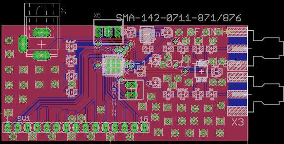
ADC Board Layout
I’ve ordered the PCB for this ADC board along with several other mini-boards which would fulfill 10x10cm area. I’ve used SeeedStudio Fusion to manufacture the PCB. Their quality is very good considering you only pay 4.9$ for 10 PCB. 10 of these PCBs cost me around 16$ including shipping, which is very nice. I’ll probably reveal more of the circuits on the same board in the near future.
Conclusion
In order to find a solution for high speed data acquisition, I’ve decided to fabricate a high speed ADC board. Now, I would have to find a cheap solution to transfer its output to PC, or process it on another platform such as FPGA. As mentioned before, high speed data acquisition is an important engineering problem. If I could manage to build myself a general purpose data acquisition system, that would be great in the long run. Now I’m waiting for PCBs to arrive. Once they are here, I’ll solder them as soon as possible and continue my work.